The development of electronics has led to the placement of a large number of electronic components in a small space. To achieve this goal, Printed Circuit Boards (PCBs) are used. They are one of the most crucial components of a device because they form the skeleton of the entire electronic circuit.
In its simplest definition, PCBs are sheets of insulating material with electrical connections and soldering points designed for mounting electronic components. With this organization, we can make controlled electrical connections between them.
Just a few years ago, creating a professional PCB was associated with high costs, so enthusiasts would create their own projects by etching copper from laminate or soldering components on universal boards. Nowadays, production costs have dropped, making it more accessible for individuals to order manufactured PCBs. It is, therefore, worthwhile to take advantage of this opportunity and creatively pursue engineering ambitions. In this article, I will explain what and why we need to prepare for the PCB manufacturer to be able to create a physical board for us.
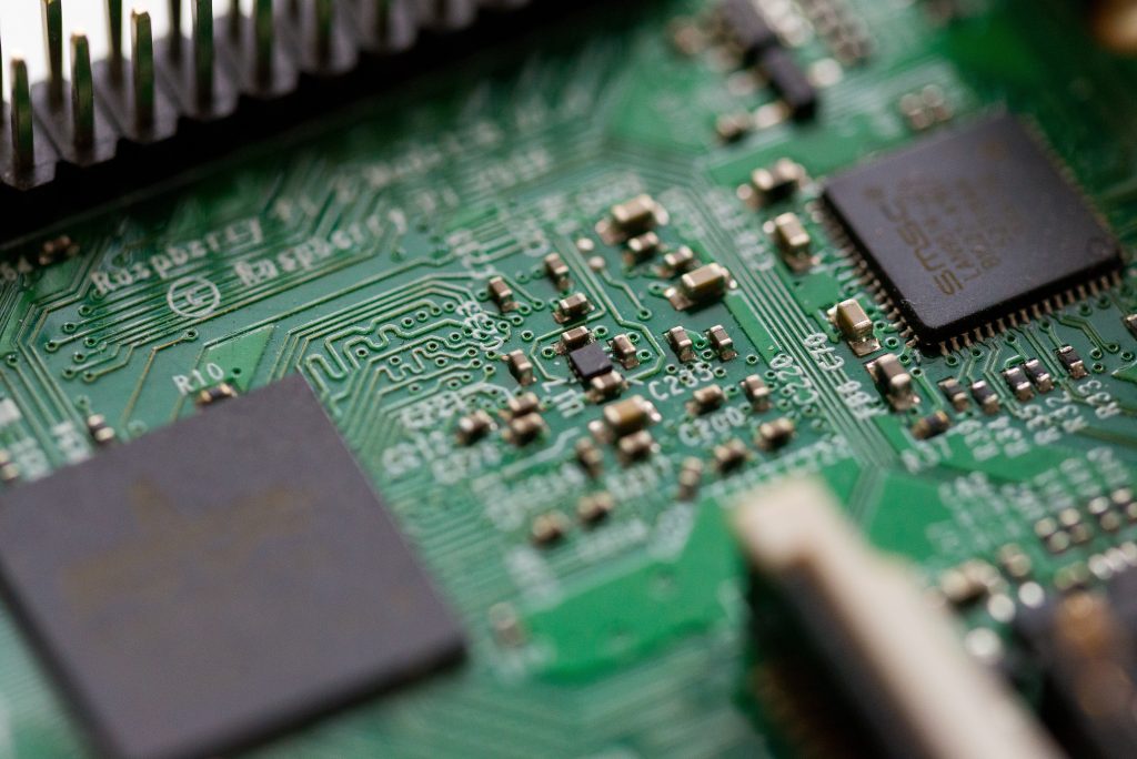
Where to start?
Having a completed schematic, it’s worth performing an Electrical Rules Check (ERC) analysis to ensure all electrical connections are correct. Before we proceed with PCB fabrication, it’s also important to establish design rules that will be enforced by the design software (e.g., Altium Designer, KiCAD, Eagle). These rules help in monitoring aspects such as trace widths and minimum isolation between high and low voltage.
This is also crucial due to potential manufacturing constraints regarding specific parameters, such as:
- minimum spacing between copper traces,
- minimum spacing between holes,
- holes diameters.
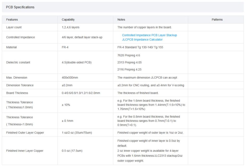
Therefore, it’s important to verify the minimum parameters that our project must meet to be producible. We perform this verification using a Design Rules Check (DRC). Picture 2 illustrates an example specification provided by a Chinese PCB manufacturer, JLCPCB.
PCB Structure
Printed Circuit Boards (PCBs) have a specific internal structure. When we talk about a “double-layer PCB,” we mean a board with 2 copper layers, while a “four-layer PCB” has 4 copper layers, and so on. Dielectric layers are usually made from glass-epoxy laminate (most commonly known as FR-4), but they can also be glass-teflon (for microwave applications) or polyamide (for Rigid-Flex boards) depending on the requirements.
During the manufacturing process, an external layer of copper is covered with a protective film, and unprotected areas are etched away, creating traces and the entire PCB structure. Unprotected copper is typically coated with regular solder or another material.
For amateur applications, solder is sufficient, but for densely packed professional boards, it’s advisable to use gold plating. This surface treatment ensures better quality, facilitates soldering, provides improved conductivity, and enhances corrosion resistance. A standard double-layer PCB will be discussed using an example of a simple PWM driver PCB designed in the KiCad software:
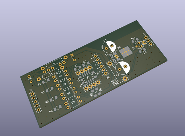
Example PCB project
A PCB consists of:
- Top/bottom silkscreen layer – it contains pin descriptions, component numbers, user information, manufacturer logos, etc.:
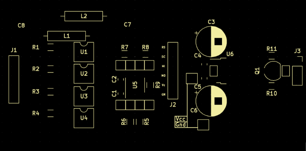
- Top/bottom solder mask – it’s a layer of lacquer (often green) that protects the PCB’s structure from external factors. The file defines areas not covered by the lacquer:

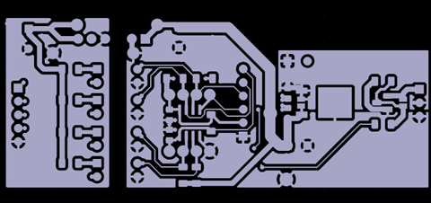
- Copper layer – this layer contains conductive material reflecting the connections of electronic components. Typically, it has a thickness of 35μm (sometimes referred to as 1oz):
- Dielectric – a non-conductive layer serving as insulation between copper layers. In standard applications, this is made from epoxy resin FR-4.
- Copper layer – another conductive layer.
- Keepout – a file containing the PCB’s outline:

- PTH (Plated Through-Hole) – a file containing coordinates and dimensions of metalized holes (vias between traces).
- NPTH (Non-Plated Through-Hole) – a file containing coordinates and dimensions of non-metalized holes (e.g., mounting holes).
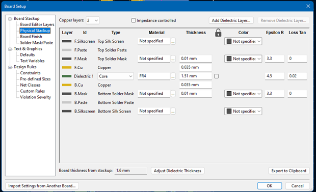
An example stack of layers in KiCad 6.0 is shown in Figure 8. Depending on the number of layers, the quantity of copper and dielectric layers will differ. If better heat dissipation is required (e.g., in power LED projects), the PCB can be made on an aluminum substrate. In this case, the copper layer is separated from aluminum using a thermally conductive insulator.
Additional Project Files
When, in addition to creating the PCB itself, we want to order component assembly, additional files are needed:
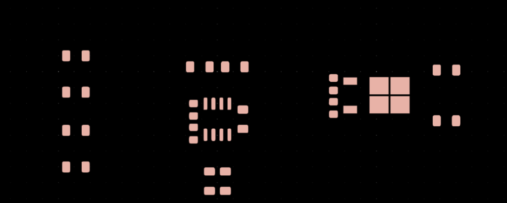
- Top paste stencil – often referred to as a stencil. It’s a metal sheet with openings used for applying solder paste:
- Bottom paste stencil – if components are mounted on both sides of the PCB, a stencil for the bottom layer will also be required,
- BOM (Bill Of Materials) – a materials list containing the designator, component value, package, side, and quantity of components of each type:

- Pick & Place – a file containing X and Y coordinates relative to the reference point and rotation information for each component, essential for automatic component placement:

Gerber File Viewers and File Sets
All the aforementioned layers are Gerber files. This is a standard vector file format used in PCB projects. It contains information about conductive traces, components, mounting holes, etc. Gerber file viewers are usually available within the software used for PCB design or online by searching for “Gerber Viewers”.
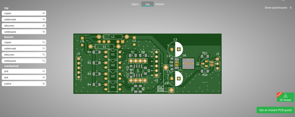
In a finalized project, you should generate a prepared set of files and drill coordinates. The absolute minimum that a PCB manufacturer should receive from us is a folder containing files reflecting the necessary layers to produce the board, i.e.,
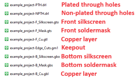
In cases where you not only want to obtain physical PCBs but also outsource component assembly, you should provide additional files, including paste stencil templates, pick and place data, and a bill of materials:

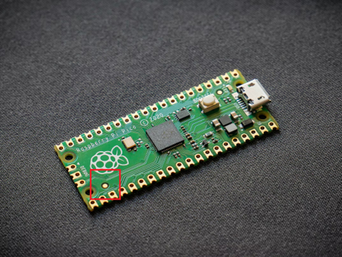
Remember to place fiducials in the corners of the PCB. These are small reference points that assist the machine performing component assembly in determining the position on the board. There should be a minimum of 2 fiducials, but ideally, 3 points, as this allows the machine to ascertain whether the board has been properly oriented. Fiducial coordinates should be included in the pick and place file.
Picture 15 shows an example appearance of fiducials (Fiducial marker):
Summary
In this article, I have discussed the process of preparing manufacturing documentation for printed circuit boards (PCBs), which is crucial for achieving high-quality PCBs. I have not only covered the types of files required for production but also explained the construction and layers of a PCB. I have provided guidance on organizing files in a folder to facilitate the work of the manufacturer and avoid errors.
Thanks to these practical tips, every engineer will have the ability to easily generate the necessary documentation for the production of high-quality printed circuit boards.
***
If you are interested in Embedded, we also recommend other articles by our experts.







Leave a comment