I guess everyone has encountered the problem of a TV screen going wild while operating an old vacuum cleaner or kitchen robot somewhere else around the house. Others have surely noticed radio reception quality drop significantly after plugging in a no-name kind of mobile phone charger into the car’s lighter socket. Electronic equipment damaged due to grid overvoltage is also no rare sight.
All these problems are related to the electromagnetic environment in which all the devices work and are caused by the lack of electromagnetic compatibility between themselves and the surrounding environment. The phenomena ruling the world of electromagnetic compatibility (EMC) are invisible to the bare eye. Those are ghosts that loiter in the less suspected places of ether. To be more precise, we are talking about sudden changes and disturbances in the electromagnetic field.
The source of the above-mentioned is the mutual impact of working devices, but the cause of their emergence needs to be addressed by designers. On the contrary, a whole army of engineers, beginning with circuit designers, layouts, and programmers and ending with EMC laboratory staff, is taking the fight to eliminate those unwanted occurrences. They are real ghostbusters, and many are in Sii resources.
Division of ghosts
First, let’s divide our ghosts in terms of:
- Source
- when they can originate inside the device and propagate to the outer world, impacting the work of other devices in the environment – we call them emissions,
- when they come from the environment and attack our device, we call them exposures, and the observed parameter of the designed device is susceptibility.
- The means of travel
- when they penetrate the surrounding electromagnetic field, we discuss radiated emissions or susceptibility,
- when they travel through connected supply and communication wires – we are talking about conducted emissions or susceptibility.
Every day, we defend, prevent, detect, and eliminate those four types of disturbances, bringing them below the safe level. The fight begins in the early conceptual phase of the design process.
Prevention in the design process

In everyday work, a hardware designer is guided mainly by fulfilling all functional and economic requirements imposed by the purchaser. Nevertheless, at every step, he needs to keep in mind that the outcome of his work will be undergoing a restrictive EMC test. At Sii, we pay much attention to the selection of electronic components, especially in terms of fulfilling emission and susceptibility standards.
Good practices
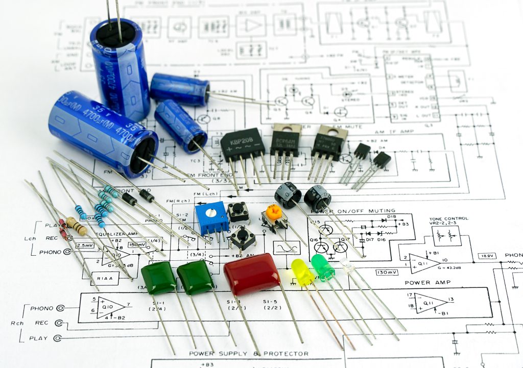
In the case of assuring immunity, the key factor is to protect the input circuits from sudden voltage drops, surges, and transients, as well as expected and differential disturbances. A good habit is to use EMI filters (often available as ready-to-use subcircuits) in the inputs and communication interfaces. It’s important to use ferrite beads on power lines and TVS diodes to protect against surges.
The ubiquity of decoupling capacitors is beyond doubt, but looking at their parameters other than capacity and rated voltage is essential. The impedance of such a capacitor often gets higher at higher frequencies, making it look more like an inductor.
Maybe it’s worth having more control over impedance to break a single capacitor into a parallel combination of two. As a rule, every parasitic parameter must be considered when putting any passive component on the schematic. Along with others, they can create unwanted resonant circuits, becoming sources of unwanted emissions or exciting under the influence of other disturbances whose sources are on the identical PCB.
DC/DC converters
DC/DC converters became very common in times of great battery power popularity. They are a potential source of problems because they quickly switch large currents. Commonly, an unwanted emission is one of the higher harmonics of the base switching frequency of such a converter.
It’s always worth digging through datasheets. They often contain guidance on what external elements to use or how the layout should look to ensure minimum emission. There are a lot of different solutions, and sometimes what works fine in one design isn’t suited for the other. On the contrary, it may cause more problems.
Clock lines
We must always take special care of all kinds of clock lines, where fast square-shaped signals are present. Even if the base frequency is not high, the presence of harmonics (due to the signal shape), especially higher, may lead to the generation of emissions exceeding safety limits.
Identifying them on the spectrum analyzer screen seems fairly simple (they represent a row of stripes separated by the base frequency distance). Still, they can be hard to reduce later on. We should always consider putting edge-blunting elements, maybe RC filters, to lengthen rise and fall times.

PCB
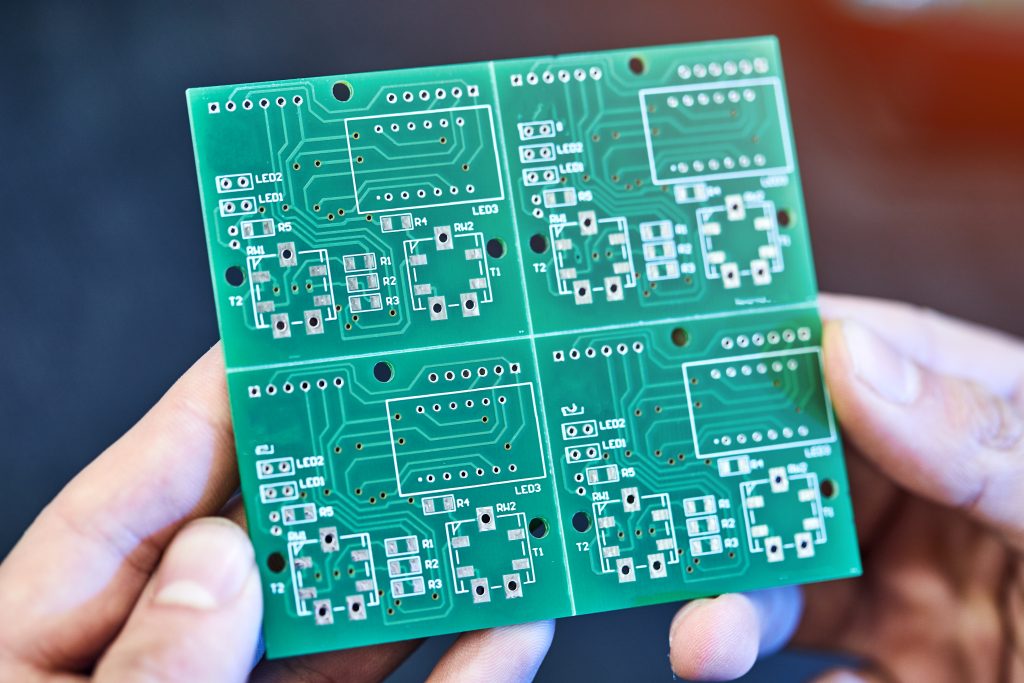
Let’s proceed to another design stage, where other EMC pitfalls await us. I’m speaking about the PCB design, i.e., the placement of elements and routing.
The first thing we should look at are the clock lines mentioned above. As a rule of thumb, they should be as short as possible and contain as little vias as possible. There should also be grounded guard tracks, stitched with ground vias, beside them. No other tracks should be routed parallel to the clock lines or placed directly beneath them. That goes especially for analog signals (as a rule, it is highly recommended to completely separate analog signals from digital signals by using different PCB stackup layers for them).
In practice, every piece of PCB track is a potential antenna that can radiate or receive disturbances, injecting them into the circuit.
The trace length is essential here because we may have created a half-wavelength antenna unwillingly. Sometimes, a slight change in track length and shape can eliminate emission problems. It matters, especially when it comes to very high frequencies. Here, even a sharp trace corner can be a source of emission; humorously speaking, the wave falls out of the corner. In that case, we should use mitered tracks and rounded corners (often seen on RF boards).
PCB vias
The same case is with vias. Each can be a radiating element, so we should minimize the number of vias. They also introduce an unwanted inductance to the track that becomes an obstacle for higher frequencies. That ids the reason decoupling capacitors should be placed close to ICs without the use of vias. In an extreme case, a via can create a resonance circuit with one of the capacitors.
That does not mean that via’s are the ills of every PCB. They play an invaluable role in routing ground shields and stitching ground planes, eliminating parasitic capacitances between different board layers.
Vulnerable PCB traces
The above-mentioned copper-bearing supply ground potential regions may be key elements in eliminating unwanted emissions. High-frequency disruption currents don’t always flow through copper traces meant for them. Sometimes, just like ghosts, they can penetrate walls of isolation and other traces, causing crosstalk and transmission interruptions. They can also choose free space to travel back to the source, causing radiated emissions.
Surrounding such traces with fills of copper and placing copper polygons beneath them will provide a short and safe way of returning with minimum impedance.
Software
And on the software side? It may seem that programmers are on the safe side and EMC ghosts aren’t a threat to them. On the contrary, a few actions regarding software can impact both emissions and the susceptibility of our design. Earlier on, we discussed the clock lines. It turns out that many microcontrollers have the feature to software control the rise and fall times of serial clock lines. Using the minimum clock frequency that satisfies the desired transmission speed is recommended.
And what about susceptibility? A good software error correction can eliminate the impact of disturbances on the transmission lines connected to the device. The same goes for software mechanisms eliminating undetermined states on microcontroller inputs.
The shield
We can go even further. Engineers from beyond the field of electronics may take part in assuring electromagnetic compatibility. The final barrier protecting the electronic circuit from unwanted ghosts and keeping the emissions from radiating to the outer world is the shielding enclosure of the device. Mechanical constructors may have some work to do here.
What seems at first a tight ‘can’ may have cracks and other imperfections that can create slot antennas. Through them, emissions may ‘leak out’ of the enclosed device. To avoid that, we should use EMC seals, usually found as stripes of rubber with metallic addition, dense copper grids, or stripes of toothed elastic metal bands. Such seals can combine the functions of EM shielding and dust and waterproofing.
If we are certain that all measures have been taken in the design process, we may introduce our device to the haunted EM environment. At first, it was in the controlled conditions of the EMC test lab. It’s a place equipped with tools of war that bear both strange names and appearances, such as the equipment of real Ghostbusters from the movie. A few words on the subject below.
Standards and methods of testing
As I mentioned earlier, the main goal of designers in the field of electromagnetic compatibility is to protect the device from the influence of the surrounding environment and ensure a safe level of emissions introduced to that environment by the device.
What level of interference can we assume is a safe one? Is it the same for every electronic device? Over the years, many different authorities came up with standards where precise emission levels (both radiated and conducted) and interferences (when it comes to susceptibility testing) that the equipment under test (EUT) should fulfill.
The standards also describe methods of testing and the necessary equipment that provide full repeatability of the test outcome, regardless of the testing site.
Different industries use dedicated standards (for example, industrial EN IEC 61000-6-1 and others from the 61000 series; automotive ISO family 11451-1 to 11451-5 and military different revisions of MIL-STD-461). The selection of appropriate standards for the designed equipment is a case, especially when the purchaser does not state that clearly. The device may have many different functionalities, which may result in the need for testing according to more than one standard. Due to different testing methods and equipment, there is no way of simply ‘translating’ the test results from one standard to another standard’s ‘language.’
Verification
After choosing a proper standard, i.e., types of tests and equipment, the EMC test lab carries them out.
The result is positive (PASS) if:
- when testing emissions (both conducted and radiated) – the level of disturbance (in the surrounding free space or the connected wires) does not exceed the standard-provided limit line, that is, a set of limit values (different for different frequency bands) that the measured signal strength should not surpass. If, at any place, the signal exceeds the limit line, the result is negative (FAIL).
- when testing susceptibility (conducted and radiated), the result is positive if the device is working stable regardless of the disturbances injected into the connecting cables or interrupting the EM field around it. The device’s state is monitored by appropriately protected testing equipment delivered by the test ordering party. In some cases, this can be substituted by observation of the device’s behavior by the lab’s staff. Any deviations are noted and may cause a negative test result. Often, the device is sent back to the producer ‘in pieces’ after being permanently damaged during tests.
Course of tests
The tests are applied to the device, but the testing setup consists of connecting supply and communication lines and wire bundles. It is also necessary to prepare testing equipment measuring and monitoring the stets of the device under test. The device should be switched on during tests in the typical activity state. If there is more than one state, the most interfering one should be selected. It is also important to remember that any hardware or firmware updates generate the need to repeat all the tests.
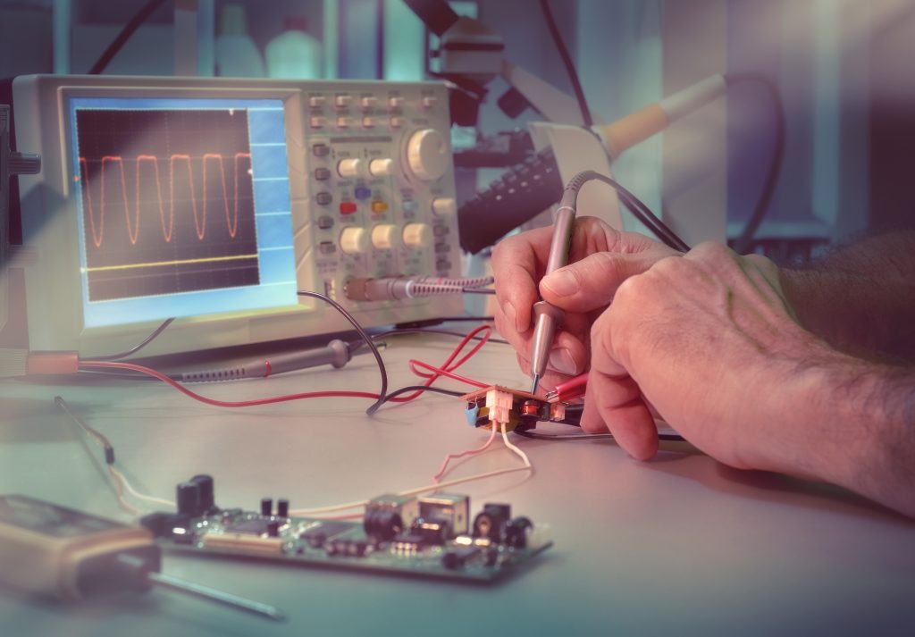
Due to the time and cost of tests conducted in authorized laboratories (due to the long waiting time), many producers test the final revisions of their products. Any modifications at the stage of authorized testing may become very expensive. That is why many producers carry out engineering tests at their facilities. By investing a moderate amount of money, we can buy a spectrum analyzer and a near-field probe set, which helps locate radiation sources on a bare PCB.
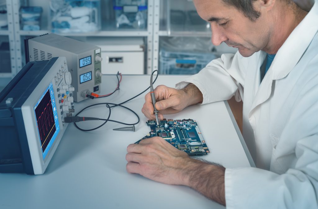
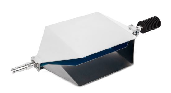
Another valuable piece of equipment is a TEM measurement chamber.
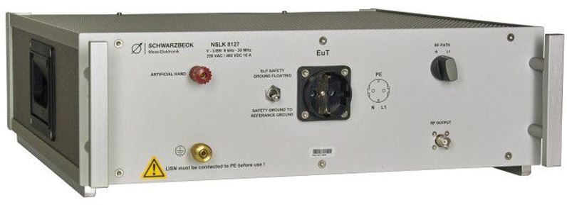
A LISN (Line Impedance Stabilization Network) is also a must-have when testing conducted emissions.
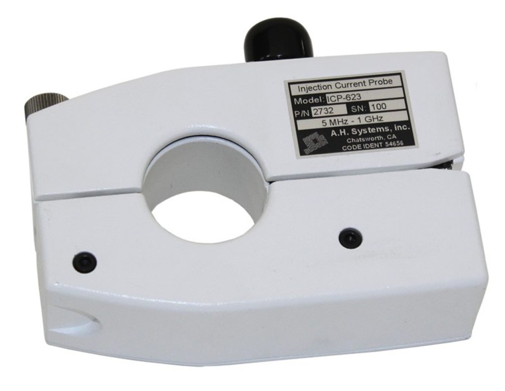
After conducting radiated emissions, susceptibility, and conducted emissions, the last step is to test for conducted susceptibility. The basic equipment is generators and injection probes or coupling/decoupling networks.
Equipped with all that stuff from the Ghostbusters movie, we may begin a crusade against those EMC ghosts. But having in mind that prevention is better (and cheaper) than cure, it is best recommended to think about EMC from the very first moments of the project’s implementation.
Conclusion
Although the matters discussed above do not exhaust the topic of EMC, which is a wide engineering field, they should shed light on the issue. I managed to present the concept of EMC and how to ensure it and test it.
We should remember that there is no escape from EMC. The requirements for the designed equipment will grow with the increase in devices sharing the same electromagnetic environment. Practice dictates thinking about EMC issues from the design assumptions.
A well-designed device does not fear the EMC ghosts. If, however, it turns out that they disturb the restful sleep of engineers, don’t panic. Who are you going to call? Call Sii, and our ghost hunters will clean up your project.




Leave a comment